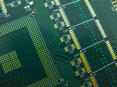
In the ever-evolving world of electronics, the demand for higher performance and miniaturization is pushing the boundaries of design. High-Density Interconnect (HDI) Printed Circuit Boards (PCBs) have emerged as a leading solution, combining efficiency with cutting-edge technology. This blog delves into the intricacies of HDI PCBs, exploring their benefits, applications, and design considerations.
What Are HDI PCBs?
High-Density Interconnect PCBs are advanced circuit boards characterized by a higher wiring density than standard PCBs. They utilize finer lines and spaces, smaller vias, and microtias, which allow for increased functionality in a smaller footprint. As the name suggests, HDI PCBs are designed to accommodate densely packed components, making them ideal for modern electronic devices that require high performance without compromising on size.
The Advantages of HDI PCBs
Space Efficiency
One of the most significant advantages of HDI PCBs is their ability to maximize space. By employing smaller components and more intricate designs, HDI PCBs can reduce the overall size of the circuit board. This efficiency is crucial in applications like smartphones, tablets, and wearables, where every millimeter counts.
Improved Performance
The intricate design of HDI PCBs allows for shorter signal paths, reducing the time it takes for signals to travel between components. This feature leads to improved signal integrity and higher performance, making HDI PCBs suitable for high-speed applications such as telecommunications and data transfer.
Thermal Management
With the increasing complexity and performance demands of electronic devices, effective thermal management is essential. HDI PCBs often feature better thermal dissipation properties due to their multilayer construction and the strategic placement of heat-generating components. This design can help prevent overheating and enhance the longevity of electronic devices.
Flexibility in Design
HDI technology offers greater flexibility in PCB design. Engineers can integrate a variety of components, including high-density chip packages and embedded passive components. This flexibility allows for innovative designs that can incorporate additional functionalities without increasing the size of the PCB.
Cost Efficiency in the Long Run
While the initial costs of HDI PCBs may be higher than traditional PCBs, the long-term benefits often outweigh these costs. The improved performance, reliability, and longevity of HDI PCBs can lead to significant savings in maintenance and replacement costs over time. Moreover, the reduced size can also lead to savings in material costs.
Applications of HDI PCBs
HDI PCBs are employed across a wide range of industries due to their unique advantages. Here are some of the most common applications:
Consumer Electronics
The consumer electronics market is one of the primary beneficiaries of HDI technology. Smartphones, tablets, and laptops often rely on HDI PCBs for their compact designs and high performance. The ability to pack more functionality into smaller devices has made HDI PCBs essential for innovation in this sector.
Telecommunications
In telecommunications, the demand for faster data transmission and improved signal integrity is relentless. HDI PCBs are crucial in high-frequency applications, such as mobile base stations and routers, where performance and reliability are paramount.
Medical Devices
The medical field increasingly relies on advanced electronics for diagnostic and monitoring devices. HDI PCBs are used in various medical equipment, including imaging devices and portable monitors, where space is at a premium, and performance must be impeccable.
Automotive Industry
As vehicles become more technologically advanced, HDI PCBs play a vital role in automotive electronics. From advanced driver-assistance systems (ADAS) to infotainment systems, HDI technology enhances the performance and efficiency of automotive electronics.
Industrial Applications
In industrial automation and control systems, HDI PCBs enable compact designs while maintaining high reliability and performance. Their robustness makes them ideal for harsh environments found in manufacturing and process control.
Design Considerations for HDI PCBs
When designing HDI PCBs, several key considerations must be taken into account to ensure optimal performance and manufacturability:
Layer Count
HDI PCBs can be built with varying layer counts, typically ranging from four to 12 or more. The layer count should be determined based on the complexity of the design and the space available. Increasing the number of layers can improve functionality but may also increase production costs.
Via Types
There are several types of vias used in HDI designs, including microtias, blind vias, and buried vias. Each type has specific applications and advantages. Microtias, for instance, are essential for connecting layers in a densely packed board. Understanding the appropriate use of each via type is critical for effective design.
Material Selection
Choosing the right materials for HDI PCBs is crucial. Materials should not only support high-density designs but also provide adequate thermal and electrical performance. Common materials used include FR-4, Rogers, and flexible materials, each offering unique properties that can affect performance.
Signal Integrity
Maintaining signal integrity is vital in HDI PCB design. Designers must consider trace width, impedance matching, and crosstalk to ensure high performance. Careful attention to these factors can minimize signal loss and improve overall functionality.
Manufacturing Capabilities
Before finalizing your design, ensure that your chosen manufacturer has the capabilities to produce HDI PCBs.
Conclusion
HDI PCBs represent the future of PCB technology, offering a perfect blend of efficiency and cutting-edge design. Their advantages, including space efficiency, improved performance, and flexibility, make them ideal for a wide range of applications in today’s high-tech world. While there are considerations to keep in mind during the design process, the benefits of HDI technology are undeniable.
As the electronics landscape continues to evolve, staying ahead of the curve with HDI PCBs can give your products a competitive edge. If you want to explore further or need expert guidance on HDI PCB design and manufacturing, click this link here now for more information. Embracing HDI technology could be the key to unlocking new possibilities in your electronic designs.


